
Talk:Transistor/Archive 4
| This is an archive of past discussions about Transistor. Do not edit the contents of this page. If you wish to start a new discussion or revive an old one, please do so on the current talk page. |
| Archive 1 | Archive 2 | Archive 3 | Archive 4 |
Origin of the name "transistor"
The Bell labs webpage Has a copy of the ballot used to determine the name of the transistor with the description of term 'transistor' given as a portmanteau of the terms 'transconductance,' 'transfer,' and 'varistor.'
The current article claims a portmanteau of the term 'transfer resistor.' I'm new to this so I thought I would ask if anyone has an opinion. — Preceding unsigned comment added by 130.63.86.178 (talk) 16:43, 24 March 2013 (UTC)
- The ballot actually says "transconductance or transfer". I have to say that varistor makes more sense to me than resistor, but I note that varistor is itself a portmanteau of variable+resistor and that transistor has entirely lost the var element so transfer+resistor in not entirely wrong. The difficulty here is going to be sourcing. There are literally thousands of RS out there verifying transfer resistor. I could find only three results on gbooks for transfer varistor, only two or which are in English. It would be some task to show that these sources are more authoritative than the thousands of others. I do not think that the appearance of transfer varistor on a ballot paper settles the matter. This is a primary source and furthermore gives no indication of the result of the ballot or whether this interpretation was adopted. A press release from Bell Labs at the time, or the appearance of the term in their jourhanl would be much more convincing. SpinningSpark 19:03, 24 March 2013 (UTC)
History_of_the_transistor#Origin_of_the_term has JRP's own words on how he named it. Dicklyon (talk) 19:28, 24 March 2013 (UTC)
Voltage Controlled Bipolar Transistor
I have edited the text where the following statement is:
“By controlling the number of electrons that can leave the base, the number of electrons entering the collector can be controlled.[24]”
It is fundamentally not correct, and perpetuates misunderstandings as to how a bipolar transistor actually works.
Before my edits are considered to be reverted, please refer to the original Gummel–Poon_model paper cited at
http://en.wikipedia.org/wiki/Gummel%E2%80%93Poon_model
A direct quote from this Gummel-Pool paper is (P.828):
“…The new charge control relation arises from the treatment of the transport equation for the carriers that pass between emitter and collector. Use is made of the fact that recombination has only a very small effect on the junction-voltage dependence of the current passing from emitter to collector (later called the dominant current component). Hence for this dependence, but of course not for the base current, recombination is neglected. A direct closed-form solution of the transport equation from inside the emitter to inside the collector is possible…”
It is noted, recombination *is* the base current. Since this base current is neglected (initially) in the Gummel–Poon method of calculating the collector current from the base emitter voltage and collector voltage it is simply not reasonable to then claim that “the collector current is *controlled* by the base current”.
The “charge control” model, by design, as shown above, calculates the base charge resulting from the applied *voltages* at the base and collector. It is noted that the base charge is not the charge flowing out of the base, but the charge in the base region, which has no direct relation to the charge flowing out of the base.
So, fundamentally the bipolar transistor is a voltage controlled device. Any base current that flows is simply a nuisance, and not any way key to transistor operation. This is clearly the opinion of some of the most noted experts (Gummel-Pool) on transistor theory.
If any editor has a more academic *reliable* source that contradicts the Gummel-Pool voltage controlled view above, and can present the basics of an actual theory as to why the bipolar transistor would be base current controlled, present it here, or please leave my latest edits alone. Kevin aylward (talk) 13:02, 27 December 2012 (UTC)
' BJT is a current controlled voltage device but JFET is a voltage controlled current device. Explain it.'
One could argue that both devices are non-linear "voltage-controlled resistors", but the usefulness of a model is based on the ease and accuracy of creating or comparing a model with reality.
After reading the comparison http://www.designers-guide.org/VBIC/documents/ted00.pdf of the old (Spice-Gummel-Poon) SGP model with new VBIC ( Vertical Bipolar Inter-Company) model developed by a group from the Semiconductor Industry, I am convinced it is the better way to forward in use of SPICE models. The precise modelling requires sequential non-linear regression and then a tolerance of parameters to std.tolerances, which is not discussed and is non-trivial. However the results are clearly, far more accurately as a result of the regression feedback. ( Praise not to Allah, but the Semi guys who developed the model.)
For example the representation of Beta or current gain, where the mountain shaped curves "almost" have a plateau in only 3 decades out 10 for Ic ( 6,7&8 ). The last two decades are a steep cliff where saturation begins and Beta drops to 10 (on most devices)
So I hope they do replace the GP model with the VBIC model in SPICE for the benefit of future application designers.
But really, both transistors are just non-linear voltage controlled resistors. There's no "active" power source inside. But the sensitivity of this behaviour makes them "active" either have good small signal gain or large signal switch properties or impedance buffers (CC mode) depend on the circuit. This "active" region, I suppose is due to the "negative" resistance behaviour, as it often observed with any plasma tube or Fear mongering god. By Dean A. (Tony) Stewart from Linkedin discussion on this topic - Phillip (talk) 20:56, 14 July 2013 (UTC)
Request for Discussion of {{Semiconductor packages}} in electronic articles
Please see the corresponding discussion thread at Wikipedia talk:WikiProject Electronics. Thanks! • Sbmeirow • Talk • 23:36, 15 December 2013 (UTC)
Package power rating table
I have cleaned up this edit from user:Magnus0re who inserted a table of transistor package power capabilities. However, I have concerns that a good deal of OR went into the construction of this table despite its heavy referencing. The "range" column seems to have been arrived at by examining a number of transistor data sheets and taking the extrema and the "approx." column by taking the average. This would make it a bad case of WP:SYNTH. I don't think packages have a minimum power rating so the range column is meaningless. More useful would be a sourced list of package maximum power ratings which one is not going to find in any transistor data sheet. SpinningSpark 11:28, 13 September 2013 (UTC)
- - You are correct in assuming that the range column have been arrived at by taking the extrema. the approx column is just that, approximate, Yes it is a created number by comparing different datasheets.
- My opinion is that the approx range may have a bad name, but I think it is true to the WP:SYNTH(no OR), because many reliable sources(hundreds, if not thousands of datasheets) exists that say that their transistor packages are capable of wattages in that range. Also the table is in line with the Neutral point of view and Verifiability, because it represents the approx number that is a more proportionate number than the maximum, (the maximum serves to promote one device while the approx serves to inform about what might be expected of a range of devices)
- The reason I included both is because this is much more useful for a person trying to select a package(rather than only maximum values, because then the engineer will be looking for the one device with max. documented power handling, which is not good.), because there is only a few rare and expensive devices that can take the maxima. (in this case only a few mosfets, not bjts.)
- On second thought maybe the Approx column should be renamed into something like "assumed median value +/- 300% accuracy, consult individual datasheet". But the purpose of the column was to put a number to what can be expected of devices in that package. Is there a better name or better way to implement such a number? Magnus0re (talk) 12:40, 15 September 2013 (UTC)
- Since you specified a range for each package, I think the approximate column should be left out as it doesn't really mean anything. A table of power range for a given package is useful information. However, the range you give is just the range you have found by looking at many data sheets. Personally, I would find that to be useful. But, you may not have actually found the extremes which is why a reliable source is needed. Also, I took the liberty of indenting your response.Constant314 (talk) 18:02, 15 September 2013 (UTC)
- I doubt that there actually exists a power rating for packages and even if it does, it is likely to be way more than any particular device. The limitation on power is dependent on many things beside the package: how the device is internally mounted and the heatsink used externally for instance. The principle limitation may not be thermal dissipation, it may be current handling capability of the device, or even the gauge of the wires or straps connecting to the top pads of the chip. I think a principle reason driving choice of package is how easily it can be mounted on a suitable size heatsink.
- I think a better approach here would be to take a suitable group of common devices and list the actual package and rating for each device. That way OR is avoided and there is no need for a whole herd of references on each line which then have to be synthesised. SpinningSpark 20:00, 15 September 2013 (UTC)
- Many packages do, in fact, have a power rating. That current rating is often similar to or sometimes *less* (!) than the number printed in the datasheet for some particular part (a number apparently printed for marketing reasons, that can't possibly be reached in any reasonable application). Since many people, even Spinningspark, have doubts on this issue, how can we improve this article to clear up those doubts? Perhaps a few words using using (a), (b)(c), and perhaps (d) as references? (This includes a "sourced list of package maximum power ratings", as originally requested by Spinningspark). --DavidCary (talk) 18:33, 14 February 2014 (UTC)
- Since you specified a range for each package, I think the approximate column should be left out as it doesn't really mean anything. A table of power range for a given package is useful information. However, the range you give is just the range you have found by looking at many data sheets. Personally, I would find that to be useful. But, you may not have actually found the extremes which is why a reliable source is needed. Also, I took the liberty of indenting your response.Constant314 (talk) 18:02, 15 September 2013 (UTC)
small-signal transistor
Several Wikipedia articles, including this one, mention "small-signal transistor". Does the transistor article need a definition of that phrase? --DavidCary (talk) 18:47, 14 February 2014 (UTC)
Semi-protected edit request on 11 May 2014
This edit request to Transistor has been answered. Set the |answered= parameter to no to reactivate your request. |
Please remove the following paragraph (added as part of edit 16:32, 30 Oct, 2006)
"Unlike bipolar transistors, FETs do not inherently amplify a photocurrent. Nevertheless, there are ways to use them, especially JFETs, as light-sensitive devices, by exploiting the photocurrents in channel–gate or channel–body junctions."
Reason: Bipolar transistors do not inherently amplify a photo current. The term "photocurrent" is not explained or defined (is this The flow of photons or electrons?). Since this paragraph Is describing a special type of FET, removing this paragraph removes a "distraction" from this more general discussion of transistors. Photosensitive FET should be covered in the FET topic.
75.4.23.63 (talk) 22:04, 11 May 2014 (UTC)
Portmanteau
@Kbrose: In this edit you wrote that transistor is a portmanteau of transresistance. It clearly isn't since a portmanteau is a blend of two or more words. Could you please provide the exact quote from your source. See History of transistor#Origin of the term for a more detailed discussion of the naming. SpinningSpark 08:13, 12 September 2014 (UTC)
The definition that portmanteau is a combination of two words is actually not accurate in linguists, I believe,where it is defined as two morphemes. In any case, I gave the explicit reference for my change, which is probably the most definitive and authoritative account and history of the Bell System ever written. That reference is also consistent with another WP article, I think it was history of the transistor. Kbrose (talk) 21:36, 12 September 2014 (UTC)
- Hi Kbrose, I was not disputing the authority of the source, my request was for an exact quote from the source. On portmanteau, the OED definition is "[a] word formed by blending sounds from two or more distinct words and combining their meanings". I think your definition of "two morphemes" is wrong, but you still need two of something to make it, not one of something. You may have been thinking of the liguistic concept of (again OED) "[a] morph which represents two or more morphemes simultaneously". That is not really relevant here, but in any case transistor is clearly not a morph since it can be broken down into its constituent morphemes. SpinningSpark 02:18, 13 September 2014 (UTC)
- Besides, a transistor is not a transresistor. Such a device would exhibit an output voltage controlled by an input current.Constant314 (talk) 03:40, 13 September 2014 (UTC)
- Many sources say that transistor is a portmanteau of "transfer resistor". However, the original transistor naming memo/ballot says, Transistor. This is an abbreviated combination of the words "transconductance" or "transfer", and "varistor". The device logically belongs in the varistor family, and has the transconductance or transfer impedance of a device having gain, so that this combination is descriptive. Dicklyon (talk) 05:20, 13 September 2014 (UTC)
- Let us look at the history: The transistor effect has been discovered 1943 in Berlin by Herbert Mataré and he used the term "Transistron" while working on the technology in Paris after 1945. It may be that the people at Bell Labs just used a variation of the term Transistron. Schily (talk) 11:07, 13 September 2014 (UTC)
- Are you sure you have that in the right order? I see various sources saying he used that term in 1948 or 1949 after realizing his device was similar to the Bell Labs "transistor". Dicklyon (talk) 14:44, 13 September 2014 (UTC)
- He filed his patent aprox. one week after the people at Bell Labs but at that time, he was already producing a small series of devices in professional cases from Telefunken (metall-ceramic tubes) that he kept from his RADAR development (noise compensating silicon duo-diodes for 3 GHz) from WW-II. Note that he owned > 90% of all pure germanium on the world at that time that was donated by Heinrich Welker. Welker created this pure germanium in the research laboratory of the air force near Munich. There is an interview with Mataré in the net from aprox. 2 years before his death. It contains a lot of information and dates. Schily (talk) 15:46, 13 September 2014 (UTC)
- But when did he use the name "transistron"? The earliest publications of that term that I find are 1949. Dicklyon (talk) 01:59, 15 September 2014 (UTC)
- It seems that the interview I have in mind vanished from the net (that one contained more about Schottky). there is however a nice interview in the appendix of a Phd work about the history of transistors (Deutsche Nationalbibliothek ref 99061915X). Mataré explains here that the word is from summer 1948 when both patents have been filed and introduced by his boss. Mataré would have used "Halbleiterverstärker". Btw: it is a pitty that WP has images of the baroque Bell labs transistor but no image from the Mataré transistor. Schily (talk) 08:49, 15 September 2014 (UTC)
- But when did he use the name "transistron"? The earliest publications of that term that I find are 1949. Dicklyon (talk) 01:59, 15 September 2014 (UTC)
- He filed his patent aprox. one week after the people at Bell Labs but at that time, he was already producing a small series of devices in professional cases from Telefunken (metall-ceramic tubes) that he kept from his RADAR development (noise compensating silicon duo-diodes for 3 GHz) from WW-II. Note that he owned > 90% of all pure germanium on the world at that time that was donated by Heinrich Welker. Welker created this pure germanium in the research laboratory of the air force near Munich. There is an interview with Mataré in the net from aprox. 2 years before his death. It contains a lot of information and dates. Schily (talk) 15:46, 13 September 2014 (UTC)
- Are you sure you have that in the right order? I see various sources saying he used that term in 1948 or 1949 after realizing his device was similar to the Bell Labs "transistor". Dicklyon (talk) 14:44, 13 September 2014 (UTC)
- Let us look at the history: The transistor effect has been discovered 1943 in Berlin by Herbert Mataré and he used the term "Transistron" while working on the technology in Paris after 1945. It may be that the people at Bell Labs just used a variation of the term Transistron. Schily (talk) 11:07, 13 September 2014 (UTC)
iron core air core
or semi conductive core> "A transistor is often composes of semi-conductors" Zinc plated Iron = 'semiconductor' rapped around a magnesium core a magnet is applied to the outer semi-conductor and the magnesium core is removed you now have a semi conductive air core transistor EMP + Hazard urName (talk) 10:26, 20 January 2015 (UTC)
please remove portuguese art
The transistor, also VLSI, was discovered and made in U.S.A. not portugal. Anyone knows the "famous electronic circuit in stone" is a large floorspace in the lofty loby of Intel HQ (Texas) which is a full circuit diagram of the 80806 processor in stone; including transistor symbols.
Take your political assertions and stick them in political articles, not in the science articles, PLEASE. — Preceding unsigned comment added by 72.219.204.96 (talk) 16:34, 24 October 2015 (UTC)
n-p-n versus p-n-p
showing the npn pnp block "doped silicon" diagrams would be allot more instructive than portuguese modern art, ie the ones in the Forest Mims electronic engineer's notebook series.
please remove the portuguese art, there is no time and room for tripe here. — Preceding unsigned comment added by 72.219.204.96 (talk) 16:26, 24 October 2015 (UTC)
- I’m rather fond of the Portuguese art. The fact that it is in Portugal isn’t important. The fact that it is laid in stone at a university outside the English speaking world attests to the global recognition of the existence and the importance of transistors and the effect that transistors have had on world culture. There is plenty of room in the article for that picture.Constant314 (talk) 18:06, 24 October 2015 (UTC)
- The one thing that Wikipedia does not have a shortage of is space. As for time, it is for readers to decide how much time is spent reading here. What we don't have time for is the kind of intolerance and prejudice you are displaying. Wikipedia is a global encyclopaedia, and that includes Portugal. SpinningSpark 18:28, 24 October 2015 (UTC)
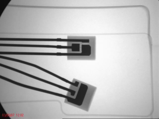
XRAY photo of Transistors
Something like this would be educational for this article, actually XRAY of all electronic parts would be very interesting for all electronic part articles on Wikipedia. If anyone has any XRAY photos with the correct "rights", please upload and add to appropriate Wiki article. Thanks! • Sbmeirow • Talk • 03:34, 18 November 2015 (UTC) : Xray of TO-92 transistor package - https://c2.staticflickr.com/4/3040/3574799585_e8270b0531_z.jpg?zz=1
- You could e-mail the Flickr uploader. I have had a good deal of success in the past with Flickr users getting them to change the licence once I explained what I wanted to do with the image. No guarantee of course, it's entirely up to them. SpinningSpark 15:12, 18 November 2015 (UTC)
- It might be more useful to get a picture with the package removed. Too bad I don't have a lens that can focus that close. Jc3s5h (talk) 17:25, 18 November 2015 (UTC)
- There is already one in the article of a Darlington transistor. I'm pretty sure that there are some more on Commons. SpinningSpark 17:44, 18 November 2015 (UTC)
- It might be more useful to get a picture with the package removed. Too bad I don't have a lens that can focus that close. Jc3s5h (talk) 17:25, 18 November 2015 (UTC)
- I am not sure whether an Xray photo is helpful as it just shows the copper contacts. If you like to show internals, you need to open a metal case or use nitric acid to remove the plastic shelf. Schily (talk) 10:46, 19 November 2015 (UTC)
Multiple-emitter ROMs
@Jc3s5h: Multiple-emitter transistors can be used in ROMs [1], but I've no idea what the OP meant by "analog". Perhaps he considers any application of BJTs to be analog? SpinningSpark 17:06, 10 December 2015 (UTC)
For those who haven't seen it, this thread is about this revert of an edit by user:Phiarc. SpinningSpark 17:10, 10 December 2015 (UTC)
- I've never heard of an analog ROM either. Jc3s5h (talk) 21:50, 10 December 2015 (UTC)
The technology was developed by Barrie Gilbert of Tektronix for the analog readout system of the 7000 series oscilloscopes. You can read about it here. The analog mask ROMs use an array of multi-emitter transistors. Data is stored in these ROMs in the number of emitters connected to the output. Similar technology was duplicated in the USSR to the best of my knowledge. However, since it is pretty niche I'm totally fine with it not being in the article. -- Phiarc (talk) 22:48, 10 December 2015 (UTC)
Need better picture of NPN/PNP symbols for infobox
Currently, there aren't very many clean images of electronic symbols available at wikimedia for use in the infobox. (Compare to the nice svg images in Resistor and Capacitor.) If anyone had any, or could produce any, that would be very much appreciated. Tpdwkouaa (talk) 23:13, 22 December 2015 (UTC)
A transistor is an amplifier or switch, not a perpetual motion engine
"John Bardeen and Walter Brattain at AT&T's Bell Labs in the United States performed experiments and observed that when two gold point contacts were applied to a crystal of germanium, a signal was produced with the output power greater than the input.[11]"--That makes it sound like the crystal added power. It could not have. The article cited actually says, "When the point of the triangle was placed onto the germanium, the signal came in through one gold contact and increased as it raced out the other." It doesn't mention that there must have been a second input providing the power for the output signal, but I assume there was. A transistor--and, I presume, that crystal--uses a small signal to modulate a larger signal. However, I don't know how the sentence should be rephrased, since the cited article is unclear on where the input power came from. Philgoetz (talk) 02:59, 18 February 2017 (UTC)
- Yes, amplifiers work by taking power from a power supply. Energy is conserved. Dicklyon (talk) 04:02, 18 February 2017 (UTC)
Introduction misleading on Lilienfeld?
The introduction looks excellent in most respects, but I feel it is a little misleading on the subject of Lilienfeld's contribution. "...conceived...by Julius Lilienfeld, and...practically implemented by...Bardeen...Brattain, and...Shockley" makes it sound like Lilienfeld did all the creative work and BBS were just his laboratory assistants. Were Bardeen, Brattain, and Shockley even aware of Lilienfeld's work? The Nobel was given to BBS, but the intro makes it sound like Lilienfeld also shared in it. L didn't even build a prototype. I think the intro should credit BBS as the inventors, but say Lilienfeld had the idea for the field-effect tran sister before them. --ChetvornoTALK 20:39, 6 March 2016 (UTC) ChetvornoTALK 20:39, 6 March 2016 (UTC)
- Yes, it's completely misleading and should be taken out. Lilienfeld's idea was a field-effect device, completely unrelated to the point-contact junction device that was actually the first transistor. Lilienfeld deserves a mention in this article, but he really was not part of the thread that led to the first transistor being made. SpinningSpark 22:45, 6 March 2016 (UTC)
- Yes, misleadingly stated. Lilienfeld's invention did come up as a big block to broad patent coverage on the transistor; Shockley tried to make a FET, but couldn't make it work at that time, due to surface charge problems; then the other guys came along and made the bipolar work. The relationship here is important, but hard to state correctly in so few words. Dicklyon (talk) 04:10, 7 March 2016 (UTC)
- When I was reading the article, I noticed the ambiguity over Lilienfeld and the Nobel Prize. I've gone and changed the wording to remove the ambiguity by making the winners' names explicit. There might be a better way to phrase it than I've done but it's an improvement. Also, don't forget our unofficial motto: "Be bold". Jason Quinn (talk) 21:10, 25 March 2016 (UTC)
- As the History of the transistor shows there was also Oskar Heil's 1934 patent on a field-effect transistor but how that figured (if at all) into the 1947 discovery is not touched on.--2606:A000:7D44:100:D884:3657:746F:E0DB (talk) 16:41, 4 April 2017 (UTC)
Recent addition regarding static induction transistor (SIT)
The statement that the SIT invented in 1950 was the first high frequency transistor or even that it was a high frequency transistor is in not supported by any of the references. What is supported is that as of the date of one reference’s publication (1996), Silicon Carbide SIT’s were faster than silicon devices. That the SIT was the fastest transistor through he 1980’s is not supported by any of the references. The references do confirm that the SIT was invented in 1950 by Watanabe and Nishizawa. Constant314 (talk) 22:19, 14 May 2017 (UTC)
- I've reverted it for now. The McCluskey source says that experimental SITs were fabricated in 1975. High frequency transistors were certainly available in the 1960s, so claiming SITs as the first is dubious at best. Maybe it was the first HF design to be studied or published, but that would need a source saying so explicitly. SpinningSpark 22:35, 14 May 2017 (UTC)
External links modified
Hello fellow Wikipedians,
I have just modified 2 external links on Transistor. Please take a moment to review my edit. If you have any questions, or need the bot to ignore the links, or the page altogether, please visit this simple FaQ for additional information. I made the following changes:
- Added archive https://web.archive.org/web/20150108082709/http://www.todaysengineer.org/2003/May/history.asp to http://www.todaysengineer.org/2003/May/history.asp
- Added archive https://web.archive.org/web/20150108082709/http://www.todaysengineer.org/2003/May/history.asp to http://www.todaysengineer.org/2003/May/history.asp
When you have finished reviewing my changes, you may follow the instructions on the template below to fix any issues with the URLs.
This message was posted before February 2018. After February 2018, "External links modified" talk page sections are no longer generated or monitored by InternetArchiveBot. No special action is required regarding these talk page notices, other than regular verification using the archive tool instructions below. Editors have permission to delete these "External links modified" talk page sections if they want to de-clutter talk pages, but see the RfC before doing mass systematic removals. This message is updated dynamically through the template {{source check}} (last update: 5 June 2024).
- If you have discovered URLs which were erroneously considered dead by the bot, you can report them with this tool.
- If you found an error with any archives or the URLs themselves, you can fix them with this tool.
Cheers.—InternetArchiveBot (Report bug) 14:30, 2 August 2017 (UTC)
Spule
I just wanted you to know that german Wikipedia has an article for "inductor" and it's not "Induktanz" but "Spule".
- Spule means "coil", not inductance. The German article does explain that coils are passive components that possess a definite inductance: Andererseits sind separate Spulen induktive passive Bauelemente, deren wesentliche Eigenschaft eine definierte Induktivität ist. SpinningSpark 12:54, 7 September 2017 (UTC)
Julius_Edgar_Lilienfeld
https://en.wikipedia.org/wiki/Julius_Edgar_Lilienfeld
"Because of his failure to publish articles in learned journals and because high-purity semiconductor materials were not available yet...."
So he didn't publish anything, and his invention was impossible, why is this person here? He should not even be in this wiki. Why don't you put Leonardo Da Vinci in here? — Preceding unsigned comment added by 73.137.94.180 (talk) 04:38, 8 December 2017 (UTC)
Number (grammar)
This edit changed "transistors" to "transistor". It appears to me the sentence requires the plural.
The edit summary stated "does anyone call bare dice 'discrete transistors' ? Undid revision 842048014 by Tom94022 (talk)) ".
I don't understand how the edit summary justifies the edit. I DO call bare dice, each containing one transistor, discrete transistors. I saw some IBM Solid Logic Technology being tested just after the discrete transistors had been assembled onto the module. (They were thoroughly obsolete when I saw them, but they had been used in some obscure peripheral or power supply, and the department that designed it never got the memo about SLT being depricated.) Jc3s5h (talk) 01:57, 20 May 2018 (UTC)
- I agree. It should be plural. Constant314 (talk) 02:17, 20 May 2018 (UTC)
Discretes such as 2N2222A are sold as bare dice (a plural I prefer to die), e.g. here. And yes bare dice are referred to as discrete transistors e.g. here. Dicklyon (talk) 01:01, 22 May 2018 (UTC)
- That should settle that issue. At least one manufacturer provides discrete transistors as bare die. Constant314 (talk) 01:41, 22 May 2018 (UTC)
- I'm still of the opinion that die is used as both singular and plural by at least some large semiconductor companies (Texas Instruments, On Semi and Analog Devices). Infineon uses dies. The distributor SemiDice use die. Micron avoids the issue by using die only as an adjective such as bare die products. Constant314 (talk) 17:27, 22 May 2018 (UTC)